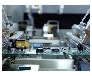
Selective welding and wave soldering are commonly used in PCB assembly proofing. However, each of these methods has its own advantages and disadvantages. Let’s take a look at selective welding and wave soldering – which one is more suitable for SMT chip processing, proofing and assembly?
Wave soldering
Wave soldering, also commonly known as reflow soldering, is carried out in a protective gas atmosphere, because it is well known that the use of nitrogen can greatly reduce the possibility of welding defects.
Wave soldering process includes:
1. Apply a coat of flux to clean and prepare the assembly. This is necessary because any impurities will affect the welding process.
2. Circuit board preheating. It’s will activates the flux and ensuring that the board is not subjected to thermal shock.
3. The PCB passes through the molten solder. As the circuit board moves on the crest guide rail, an electrical connection is established between the electronic component leads, PCB pins and solder.
Wave soldering is extremely advantageous in mass production, but it also has its own series of disadvantages, mainly including:
1. the consumption of solder is very high
2. it consumes a lot of flux
3. Wave soldering uses a lot of power
4. Its nitrogen consumption is high
5. Wave soldering needs to be reworked after wave soldering
6. It also requires cleaning the wave soldering hole tray and welding components
7. In a word, the cost of wave soldering is very high, and the operating cost is considered to be nearly five times that of selective welding.
Selective welding
Selective welding is a kind of wave soldering, which is used to upgrade the SMT processing equipment assembled with through-hole components. Selective wave soldering can produce smaller and lighter products.
Selective welding process includes:
Application of flux on components to be welded / circuit board preheating / solder nozzle for welding specific components.
Advantages of selective welding:
1. Flux is applied locally, so there is no need to shield some components
2. No flux is required
3. It allows you to set different parameters for each component
4. No need to use expensive aperture wave soldering trays
5. It can be used for circuit boards that cannot be wave soldering
6. Overall, its direct advantage to customers is low cost
Therefore, how to choose a suitable PCB assembly processing method needs to be comprehensively evaluated by customers according to the characteristics of products.
PCBFuture provide all inclusive PCB assembly services, including PCB manufacturing, component sourcing and PCB assembly. Our Turnkey PCB service eliminates your need to manage multiple suppliers over multiple time frames, resulting in increased efficiency and cost effectiveness. As a quality driven company, we fully respond to the needs of customers, and can provide timely and personalized services that large companies cannot imitate. We can help you avoid the PCB soldering defects in your products. For more information, please email to service@pcbfuture.com.
Post time: Apr-08-2022


