1. Finger Plating
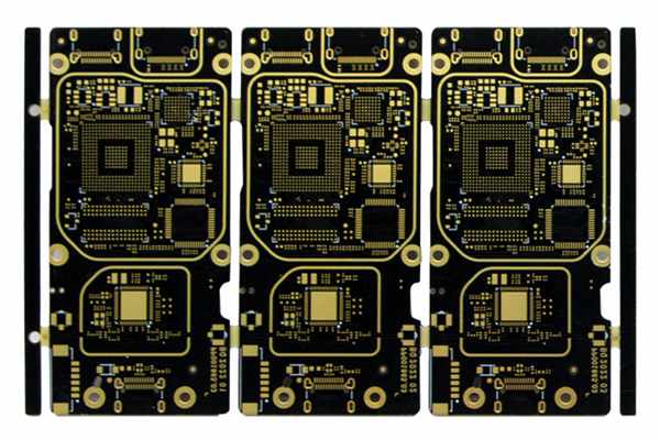
In PCB proofing, rare metals are plated on the board edge connector, board edge protruding contact or gold finger to provide low contact resistance and high wear resistance, which is called finger plating or protruding local plating. The process is as follows:
1) peel off the coating and remove the tin or tin lead coating on the protruding contact.
2) rinsing with water.
3) scrub with abrasive.
4) activation diffuse in 10% sulfuric acid.
5) nickel plating thickness on protruding contact is 4-5 μ m.
6) Clean to remove mineral water.
7) disposal of gold soaking solution.
8) gold plating.
9) cleaning.
10) drying.
2. Via plating
There are many ways to set up a qualified electroplating layer on the hole wall of the substrate drilling, which is called hole wall activation in industrial applications. The commercial consumption process of its printed circuit requires multiple intermediate storage tanks, each of which has its own control and maintenance requirements. Via electroplating is the subsequent necessary manufacturing process of the drilling manufacturing process. When the drill bit drills through the copper foil and its underlying substrate, the heat generated condenses the insulating synthetic resin that constitutes most of the substrate, and the condensed resin and other drilling debris accumulate around the hole and are coated on the newly exposed hole wall in the copper foil, and the condensed resin will also leave a layer of hot axis on the hole wall of the substrate; It shows poor adhesion to most activators, which requires the development of a kind of technology similar to the chemical action of stain removal and corrosion back.
A more suitable method for PCB proofing is to use a specially designed low viscosity ink, which has strong adhesion and can be easily bonded to most hot polished hole walls, thus eliminating the step ofetchback.
3. Roller linked selective plating
Pins and contact pins of electronic components, such as connectors, integrated circuits, transistors and flexible printed circuits, are selectively plated to achieve good contact resistance and corrosion resistance. This electroplating method can be manual or automatic. It is very expensive to stop selective plating for each pin individually, so batch welding must be used. In choosing the plating method, first coat a layer of inhibitor film on the parts of the metal copper foil that do not need electroplating, and only stop electroplating on the selected copper foil.
4. Brush plating
Brush plating is an electrostacking technology, which only stops electroplating in a limited area and has no impact on other parts. Usually, rare metals are plated on selected parts of the printed circuit board, such as areas such as board edge connectors. Brush plating is more widely used in electronic assembly workshops to repair waste circuit boards.
PCBFuture has build our good reputation in the full turnkey PCB assembly service industry for prototype PCB assembly and low volume, mid volume PCB assembly. What our customers need to do is send the PCB design files and requirements to us, and we can take care of the rest of work. We are fully capable of offering unbeatable turnkey PCB services but keeping total cost within your budget.
If you looking for a ideal Turnkey PCB assembly manufacturer, please send your BOM files and PCB files to sales@pcbfuture.com. All your files are highly confidential. We will send you an accurate quote with lead time in 48 hours.
Post time: Dec-13-2022


